


Quick analysis of the A6 SoC photos from the iPhone 5 launch event tells us all we need to know about the memory interface, speed and bandwidth of the new platform. As always, the A6 features a PoP stack combining the SoC itself and its DRAM. The package-stacked DRAM helps save space, which comes at a premium inside a device as small as a smartphone. PoP stacks are quite common in all modern smartphones.
Apple thankfully didn’t obscure the details of its A6 slide at the launch event, which gave us a Samsung part number: K3PE7E700F-XGC2. Through crafty navigation of Samsung’s product guide, Brian Klug got us the details. The K3P tells us we’re looking at a dual-channel LPDDR2 package with 32-bit channels. The E7E7 gives us the density of each of the two DRAM die (512MB per die, 1GB total). The final two characters in the part number give us the cycle time/data rate, which in this case is 1066MHz.
Plug all of that into our memory bandwidth scaling chart and you get this:
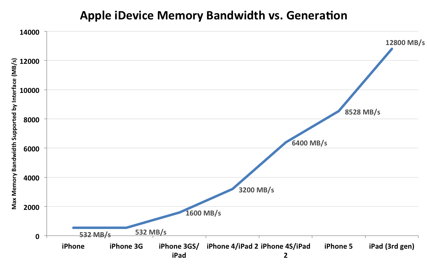
Roughly 33% more peak memory bandwidth than the iPhone 4S, which can definitely help feed the faster GPU and drive the higher resolution display. Many vendors have been shipping LPDDR2-1066 so there’s nothing too surprising here. There’s understandably less bandwidth than in the 3rd gen iPad of course as the display/GPU requirements aren’t nearly as high.
There’s more than just memory clocks that will impact memory bandwidth here. It’s unclear whether the A6 improves the memory controller Apple deployed in the A5. ARM architectures (especially in the A9 generation) have typically struggled getting good memory bandwidth efficiency. We’ll have to see what happens with the A6.
Via: Anand Tech
More: Engadget, Gizmodo, CNET, MacDailyNews, Liliputing, MacRumors,PhoneArena, AppleInsider, Engadget, iPhone in Canada Blog and 9to5Mac